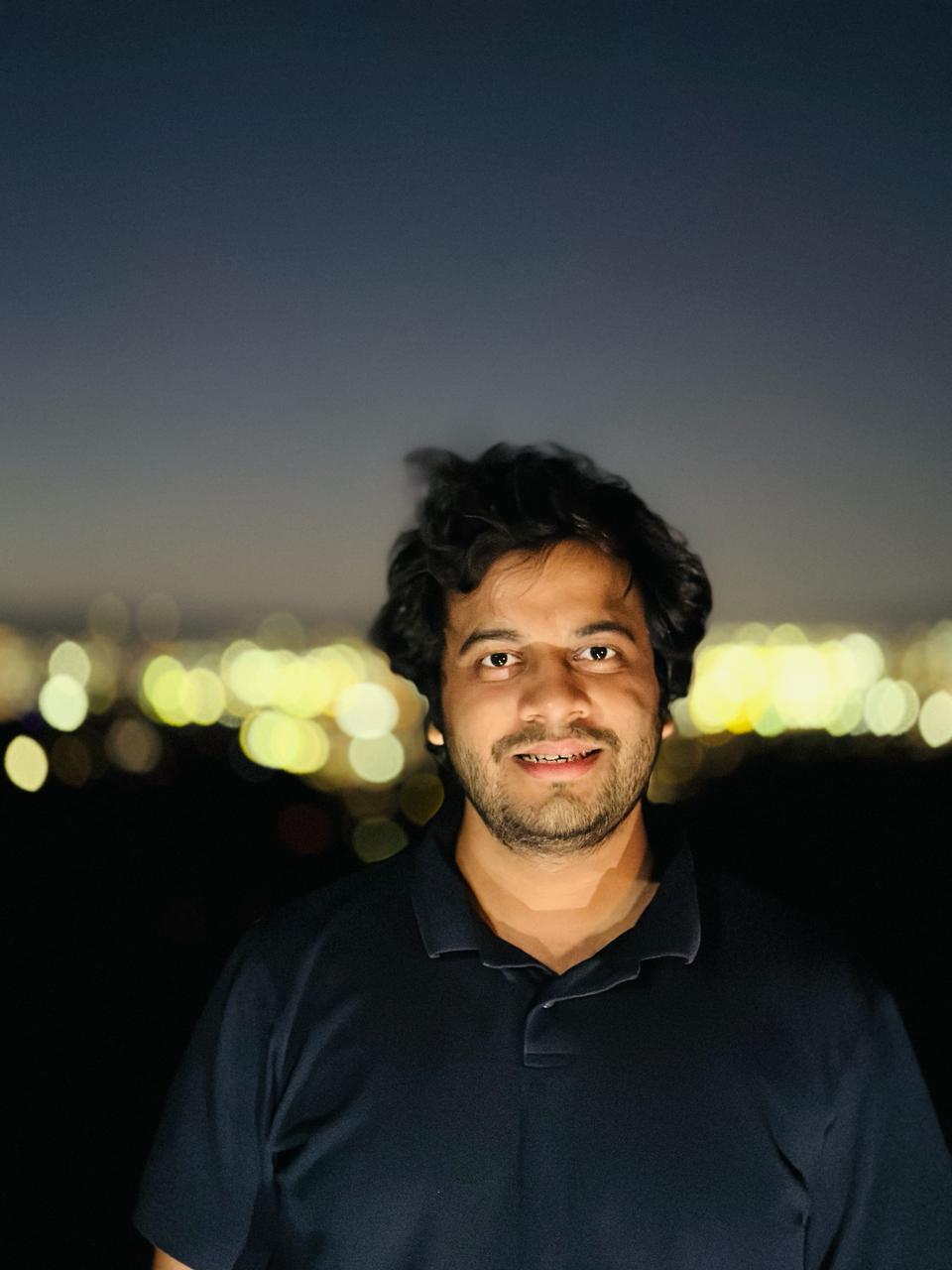
Sudhanshu Sharma
 |
Masters Student at The University of Southern California |
About
Sudhanshu was born and raised in India. He earned his Bachelor's degree in Electronics and Communication Engineering in 2019 from the National Institute of Engineering, Mysore (NIE). Throughout his undergraduate studies, he spent nearly three years as a Research and Development intern, primarily focusing on the development of Embedded Systems for AR/VR technologies.
In 2019, after completing his bachelor's degree, Sudhanshu joined MMRFIC as a Digital Signal Processing System Engineer. During his tenure, he worked on developing Beamforming techniques, Error-correcting codes, and GPS receiver algorithms.
In late 2020, he joined IIT Kanpur as a Senior Project Associate (5G Indigenous Testbed) to develop 5G physical layer algorithms for sub-6 and mm-wave frequencies.
In 2021, Sudhanshu began pursuing his Master's degree in Electrical Engineering at the University of Southern California (USC), Los Angeles, with a specialization in Wireless Communication and Signal Processing. At USC, he is also affiliated with the WIDES Lab as a Research Assistant, working on two projects: one involving joint communication and sensing using 5G NR signals, and another focused on developing low-power terahertz communication systems for brain implants.
After completing his Master's degree at USC, Sudhanshu joined Apple as a 4G/5G Cellular Performance Engineer. In this role, he focuses on optimizing the performance of cellular communication systems, ensuring high-quality connectivity and reliability for Apple's wide range of products.
News
In Spring 2023, Sudhanshu worked with NXP Semiconductors as Wireless System Intern.
In Summer 2022, Sudhanshu completed an internship at Apple Inc. as a Cellular Intern.
-
The Prime Minister of India praised the 5G testbed and standardization work at IIT Kanpur during the 2021 Convocation, where Sudhanshu contributed. [Link]
-
India is set to roll out 5G services, with Sudhanshu contributing to the development of algorithms for the downlink shared channel. [Link]
Education
Aug. 2021 - May 2023
Masters in Electrical Engineering University of Southern California, Los Angeles, United States. [Course Work]Aug. 2015 - Jul. 2019
Bachelor of Engineering (B.E.), Electronics and Communication Engineering, NIE Mysuru, India.
Worked with


|
LAST UPDATED : January'23